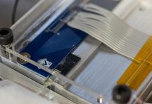
Research led by Monash University, RMIT and the University of Adelaide has developed an accurate method of controlling optical circuits on fingernail-sized photonic integrated circuits.
The development, published in the prestigious international journal Optica builds on the work by the same team who recently created the world’s first self-calibrated photonic chip.
Photonics, or the use of light particles to store and transmit information, is a burgeoning field, supporting our need to create faster, better, more efficient and more sustainable technology.
Programmable photonic integrated circuits (PICs), offer diverse signal processing functions within a single chip, and present promising solutions for applications ranging from optical communications to artificial intelligence.
Whether it’s downloading movies or keeping a satellite on course, photonics is radically changing the way we live, revolutionising the processing capability of large scale equipment onto a chip the size of a human fingernail.
Earlier this year, researchers at Monash University, RMIT and the University of Adelaide developed an advanced photonic circuit which could transform the speed and scale of photonics technology. However, as the scale and complexity of PIC’s grows, the characterization, and thus calibration, of them becomes increasingly challenging.
“We’ve added a common reference path to the chip, which enables stable and accurate measurements of the lengths (phases, time delays) and losses of the ‘workhorse’ paths,” says Monash University research fellow, Professor Mike Xu.
“By inventing a new method, the fractional delay method, we have been able to separate out the wanted information from the unwanted making for more precise applications.”
Previously chips have been measured/calibrated by connecting to complex and expensive external equipment (called a vector network analyser); however, the connections to it introduce phase errors, caused by vibrations and temperature changes. By putting the reference on the actual chip, the measurement is immune to these phase errors.
“In our earlier work we used the “Kramers Kronig” method to remove unwanted errors from desired measurements, but the fractional method requires far less optical power for calibration for a given accuracy,” says Professor Arthur Lowery, ARC Laureate Fellow from the Department of Electrical and Computer Systems Engineering at Monash University.
Adding: “This means that we can get reliable measurements of the chip’s status, so are able to accurately program it for a desired application, such as pattern recognition in an optical computer, or squeezing extra capacity from an optical communications network.”
This work complements research that began in 2020 with the development of a new optical microcomb chip, which was able to transfer 30 terabits per second, three times the record data for the entire National Broadband Network.
In the next phase of development, within the newly-announced ARC Centre of Excellence for Optical Microcombs and Breakthrough Science (COMBS), this research team will be exploring how photonic chips can use many wavelengths to achieve ultrafast information processing and machine intelligence.
“The complexity of photonic integrated circuits is rapidly increasing, requiring a breakthrough to be able to calibrate and control them. The technique we developed overcomes this challenge, ensuring that the circuits can robustly be used for applications such as pattern recognition.” says Dr Andy Boes from the University of Adelaide.
Professor Arthur Lowery, Professor Arnan Mitchell and Dr Andreas Boes are Chief Investigators at ARC Centre for Excellence, COMBS Collaboration for Optical Microcombs for Breakthrough Science (COMBS).


