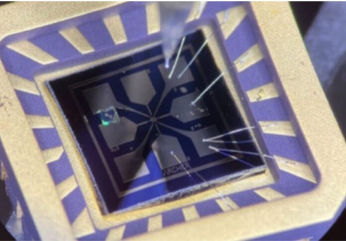
Semiconductor manufacturer Archer Materials said it is proceeding to wafer-scale quantum electronic device fabrication with the development of its 12CQ chip.
In an ASX announcement today, Archer CEO Mohammad Choucair said the company is making “considerable progress” in the development of the 12CQ technology, with its technical achievements delivering a strong basis for pursuing external engagement with tier-one semiconductor companies.
Wafer-based functional chips are crucial to the development of the 12CQ technology and will help Archer develop mobile-compatible quantum processing that can be easily integrated into modern electric devices.
According to Archer’s latest update, during the past few months, the company kickstarted technical programs of low-temperature (cryogenic) characterisation of quantum electronic devices (QEDs) necessary for the development of qubit readout and control mechanisms in Archer’s chip-based quantum logic devices.
It also partnered with researchers at EPFL to create second-generation, unique integrated chip designs for the potential complex spin manipulation of Archer’s qubit material.
The new chips are being manufactured in a semiconductor foundry located in Europe and are expected to go through testing, optimisation, and application in 2023.
In November 2022, Archer said powerful supercomputer simulations provided the most accurate understanding of Archer’s unique 12CQ qubit material to date, which is a metallic-like nanocarbon. The discovery is currently under a routine peer-review process, with publication expected in the second half of 2023.
Meanwhile, Archer said it has now obtained access to a local cutting-edge cryogenic quantum device measurement laboratory and commercial technical programs of cryogenic characterisation QEDs.
This is despite the sector’s scarcity of available and accessible world-class facilities to perform the sophisticated quantum measurements required for 12CQ chip development.
Archer is also eyeing a potential breakthrough in the foundry packaging of the 12CQ chip architecture, with the company’s engineers developing an encapsulation method for the 12CQ qubit chips that could create an artificial vacuum that would enable devices to be operated in ambient conditions.
“Initial outcomes of the packaging development indicate cleanroom processing is compatible with standard semiconductor foundry methods while maintaining coherence times. This means the approach has the potential for technology translation to industrially scale Archer’s 12CQ qubit chip architecture,” Archer Materials said in its update.


