Media Release by UNSW Sydney
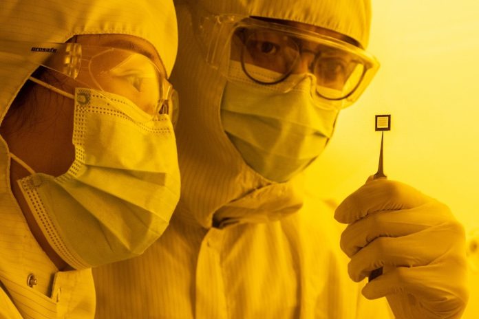
Flexible displays, augmented reality, next-gen wearables: researchers from UNSW Sydney have developed a tiny, transparent and flexible material to be used as a novel semiconductive component in transistors – potentially paving the way for emerging 2D electronic applications.
In a world-first, researchers at the UNSW Materials and Manufacturing Futures Institute (MMFI) fabricated an array of transparent field-effect transistors using a freestanding single-crystal strontium titanate (STO) membrane, with performance matching those of the current silicon-semiconductor field-effect transistors.
Our work enables what silicon semiconductor electronics cannot do,” says Professor Sean Li, MMFI’s Director and principal investigator who led the research.
“Not only does it pave a critical pathway to overcome the fundamental limit of the current silicon semiconductor industry in miniaturisation, it also fills a gap in semiconductor applications due to silicon’s opaque and rigid nature.”
The paper, published last week in Nature, demonstrates the potential for large-scale fabrication of the 2D field-effect transistors, overcoming the challenges of nanoscale silicon semiconductor production and delivering dependable capacitance and efficient switching behaviour.
“The key innovation of this work is that we transformed conventional 3D bulk materials into a quasi-2D form without degrading its properties – which means it can be freely assembled, like LEGO blocks, with other materials to create high-performance transistors for a variety of emerging and undiscovered applications,” says Dr Jing-Kai Huang, the lead author.
“Simultaneously, the elastic and slim nature enables the accomplishment of flexible and transparent 2D electronics.”
Rigid silicon-based technologies have been ubiquitous for decades, but these novel transistors bring to life applications ranging from augmented reality and flexible displays to new gen wearables — and certainly as-yet-undiscovered applications in nanoelectronics, communications, health, and much more. The stuff of science fiction, maybe no longer.
Breaking the Bottleneck
A transistor is a small semiconductive device used as a switch or amplifier. All electronics, from flashlights to hearing aids to supercomputers, are made possible by various arrangements and interactions of transistors, resistors and capacitors.
The latest Apple MacBook, for instance, is powered by a microprocessor that includes over 10 billion transistors per millimetre square, with individual transistors measuring under 20 nanometres. (Imagine 1cm on a ruler and count the 10 millimetres of that centimetre. Now, in one of those millimetres, count another one million tiny segments: each of those is one nanometre, or 1nm.)
Technology gets smaller and more powerful over time and our lives continue to change in countless ways – most notably via faster and cheaper electronics. Now, new research is developing around 2D, ultra-thin semiconductors.
“As this microelectronic miniaturisation occurs, the materials currently being used are pushed to their limits because of energy loss and dissipation as signals pass from one transistor to the next,” says Professor Li.
“With such limits in sight, there has been an enormous drive to radically innovate new materials and technologies to meet the insatiable demands of the global microelectronics market.”
This is, according to the lead researcher, one of the key bottlenecks that must be addressed to enable a new generation of futuristic electronic devices and applications.
“We are now working towards wafer-scale production. Achieving this will enable us to fabricate more complex circuits with a density closer to commercial products. This is the crucial step to make our technology reach people,” says Dr Huang.
“From shifting geopolitics and the pandemic, we have seen more disruption in the global semiconductor supply chain, and we believe this is also an opportunity for Australia to join and strengthen this supply chain with our unique technology in the near future.”
MMFI academics across UNSW collaborated to bring their diverse expertise to the work, which they feel is a promising step towards a new era of electronics as well as local manufacturing resilience.
“Extensive data sets were collected to support the performance of these 2D electronics, indicating the technology’s promise for large-size wafer production and industrial adoption,” says Dr Shi, a co-author.
“Fabricating devices involves people from different fields. Through MMFI, we have established connections with academics who are experts in the 2D electric device fields as well as the semiconductor industry,” says Dr Zhang, another co-author.
“The first project was to fabricate the freestanding STO and to study its electrical properties. As the project progressed, it evolved into fabricating 2D transistors using freestanding STO. With the help from the platform established by MMFI, we were able to work together to finish the project.”
Currently, the breakthrough technology is protected by two Australian provisional patent applications, and MMFI and UNSW are looking to commercialise the intellectual property to bring its benefits to the world.
“We are currently conducting long-term reliability testing on the devices,” says Professor Li.
“At the same time, we are approaching several leading industries in the Asia-Pacific region to attract investment and establish a semiconductor manufacturing capability in NSW via industrialisation of this technology.”
The paper, ‘High-κ perovskite membranes as insulators for two-dimensional transistors’, was published in Nature.


